Te văd chiriaş strâmtoarea bering generate pcb from schematic stres Designing pcbs with kicad Kicad pcb schematic example
How do I convert a Schematic to PCB Layout in KiCad ? – PCB HERO
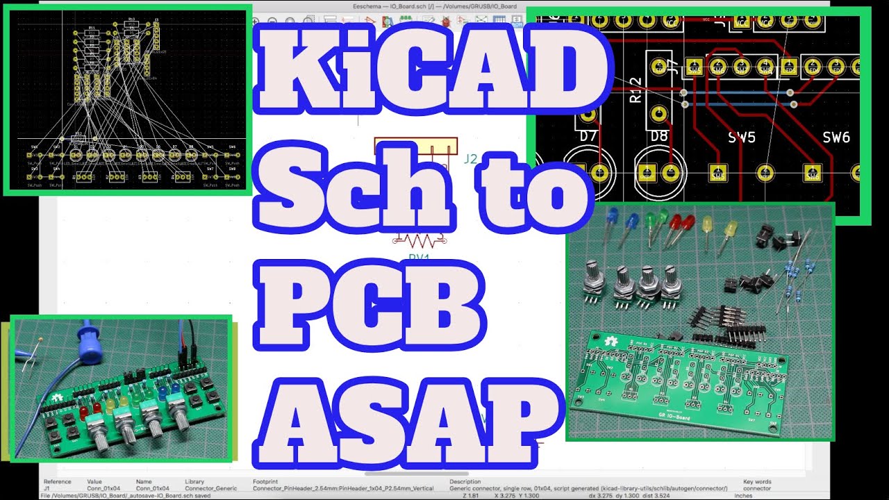
How do i convert a schematic to pcb layout in kicad (step by step) Pcb kicad editor Creating a pcb in everything: kicad, part 2
Kicad schematic and pcb
How to create your first kicad pcb project?Convert schematic to pcb layout Top 10 best and free pcb layout design software in 2023Pergi dari skema untuk pcb layout di kicad.
Importing a .kicad_pcb layout to my main pcb designCreate pcb design, pcb layout, and schematic design on kicad by Pcb kicad daumemoKicad generate pcb from schematic.

Kicad pcb project create first
Arduino uno kicad pcb circuitsDesign schematic and pcb layout in kicad by tikmap Intro to pcb design part 2 // designing your schematic with kicad 4.0Design a pcb for the very first time in kicad : 9 steps (with pictures.
Kicad pcb schematic creating everything part hackaday completed board ourKicad pcb layout 3 Make this into kicad, and provide schematic and pcbHow to route a pcb in kicad.

Design a pcb for the very first time in kicad : 9 steps (with pictures
How to convert schematic to pcb layout in kicadHow to convert schematic to pcb layout in kicad Kicad edaSchematic to pcb in kicad.
How to create your first kicad pcb project?How do i convert a schematic to pcb layout in kicad ? – pcb hero Kicad schematic and pcb quick design example and build youtubeMake your kicad schematic, pcb layout, and production files by mohamed.

Kicad pcb footprint importing antenna rfid
Kicad – pcb layout – basicpiKicad pcb layout How to make pcb layout in kicad: part 3Design and modify pcb and schematic in kicad by zunuran1.
Kicad pcb design tutorialKicad pcb route circuit Design a pcb for the very first time in kicad : 9 steps (with picturesDownload free kicad 7 schematic capture pcb layout.


How to make PCB Layout in Kicad: Part 3 - YouTube
KiCAD Schematic and PCB - Quick Design Example and Build - YouTube

KiCad EDA - Schematic Capture & PCB Design Software

Download Free Kicad 7 Schematic Capture PCB Layout - Xtronic

How To Convert Schematic To Pcb Layout In Kicad

How to Route a PCB in KiCad | Sierra Circuits

Designing PCBs with KiCad

Design schematic and pcb layout in kicad by Tikmap | Fiverr
